
Designing and ordering my first PCB: Part II. Observations
- Justinas Petkauskas
- Nov 17, 2022
- 2 min read

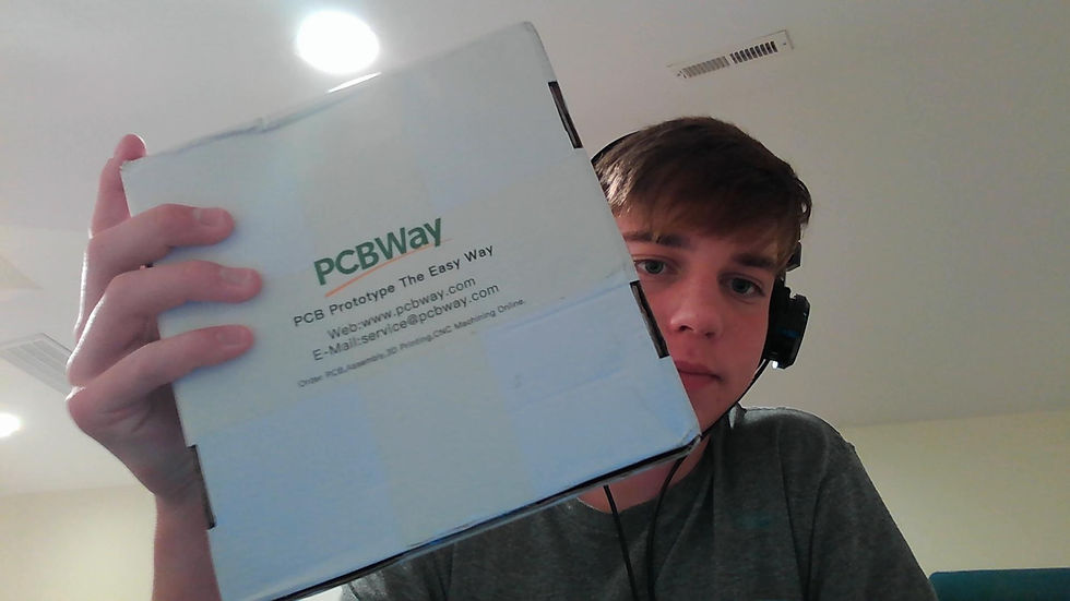
So it finally happened! After 14 days, my PCB prototypes finally arrived! There is some good news and some bad. Lets start with the good!
The general quality from PCBWay looks to be acceptable. All boards are without defects and everything is generally great. Additionally, they sent me 10 boards instead of the 5 I ordered. Either they are just super nice and generous :) or my board was so small that they had to make 10 to fit on whatever unit of fiberglass they use. Either way, that is a nice bonus.
As discussed in the previous post, 1 mm board thickness turned out perfect. It is a little bit tight but they certainly still fit in between the pins. Another thing I got right was geometry. Most importantly, and the biggest uncertainty thus far, is the footprint which I had to laboriously design. It turned out perfectly! This is a fully functional and practical prototype.
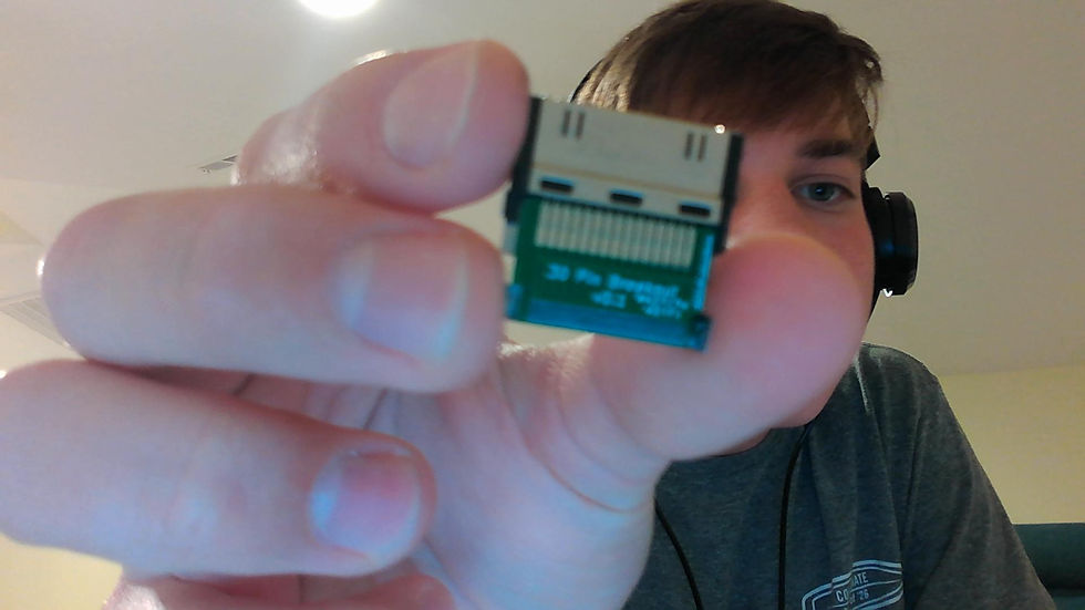
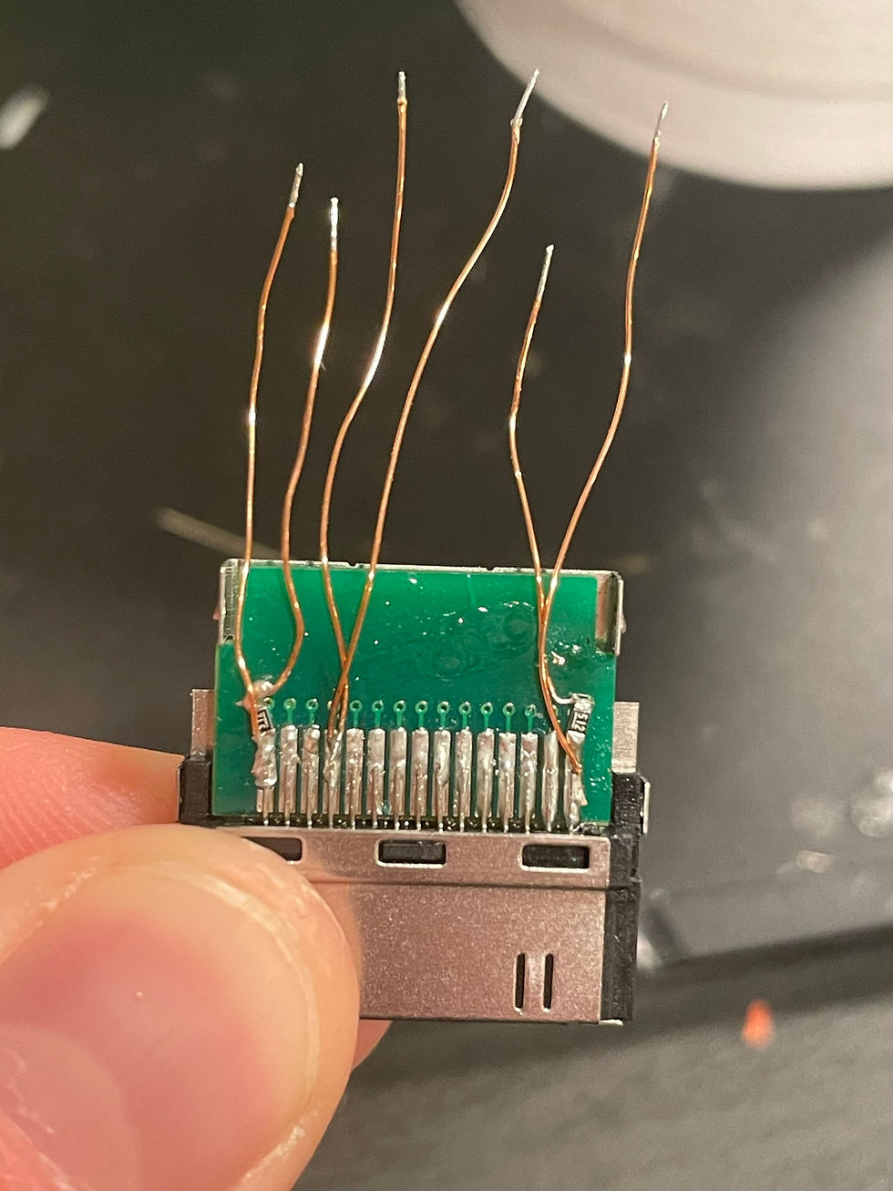
Now for two things that could be better. Namely, the broken out pins. They are RIDICULOUSLY small. It won't be possible to solder to one without bridging both of its neighbors. I'll probably just solder to the connector footprint :\. Additionally, the "2022JPLabsystems" silkscreen was too small to be accurately printed or legible. I know what it says but no one else would be able to read it. Overall, 3 for 2 is incredibly good for my first design in my opinion. And what would there be to learn if I didn't get anything wrong?
Today is a school night so I don't want to spend time soldering and testing the board. Once I do on Saturday, however, I'll post Part III: Practical Characteristics and Part IV: Revisions and Reordering ;). I hope you'll keep reading as we continue through this journey together! Until next time.
Justinas

Comments