
Designing and ordering my first PCB: Part I. The process and decisions
- Justinas Petkauskas
- Oct 31, 2022
- 2 min read

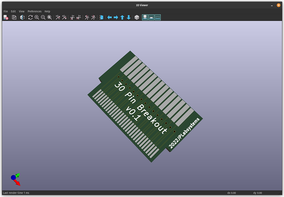
For a while now, I have been thinking about what I could do with these 30 pin connectors which I bought a few months ago. The original intent was to hand solder wires to the tiny pins of the connector to make a 3D printed iPod dock. However, problems in identifying and soldering to the pins made this difficult. I did some open source intelligence to find out what others have done.
u/oxyll of reddit has been working on incredible iPod mods for ages. One of which is a firewire/USB adapter that serves the same function as the invaluable cable. In this project, among other things, oxyll uses a PCB with the 30 pin connector. They were also kind enough to provide gerber files for their design. For those who are unaware, gerber files are the standardized files used for PCB fabrication.
So I hatched a plan. I would design my first ever PCB using the footprint from oxyll's board and break out the pads on the same board. Easier said than done, however.
The first decision was which EDA to use. I have tried Fusion Eagle, EasyEDA, and Circuit Studio before, but my favorite is certainly KiCad. It is easy to learn and use, and it is also open source and works on Linux. So I fired up KiCad, opened a new project, and created a new PCB. (A schematic was not necessary due to the board's simplicity.)
The first step was to create a footprint for the component, since the part is not widely used and oxyll's gerber files were not easily copyable. I painstakingly measured pin width, pitch, height, and other variables to generate a footprint in the KiCad footprint creation tool. After inserting the footprint into the design, I haggled with vias, board outlines, tracks, and silkscreen to create the perfect board.

After I thought I was done, I went through the export generation process and ran the DRC. (design rules checker) Only to find 32 errors on my tiny, simple board. Most had to do with my footprint intersecting with the edge cuts line, however, and were easily resolved.
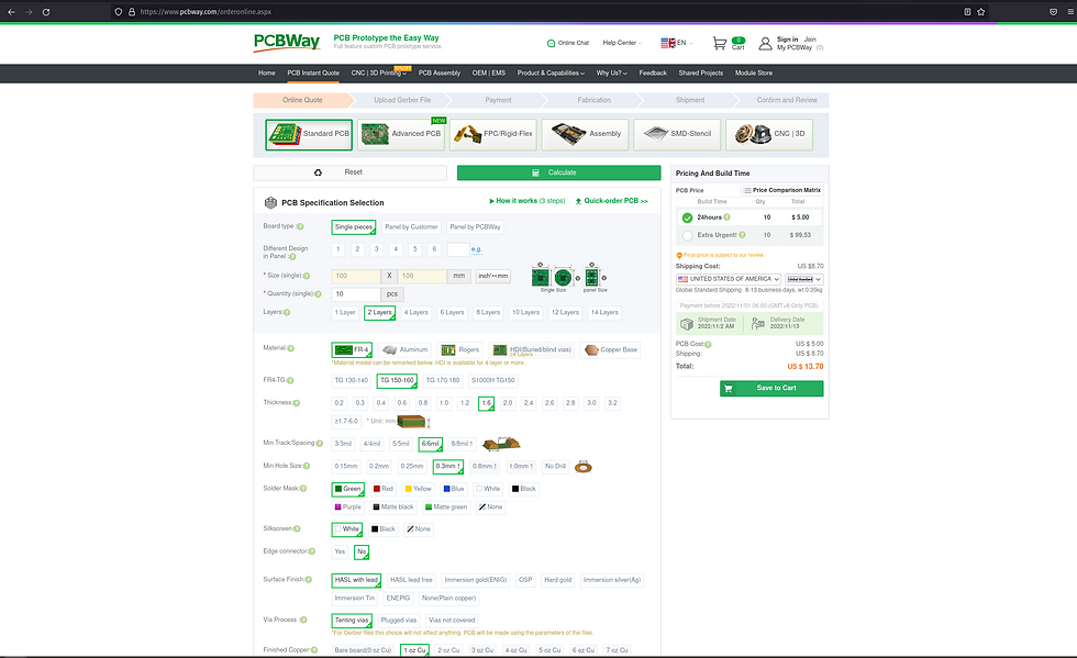
The next step was to export it and send it to a fab house. This is another big decision which had to be made. If you are a maker, whether you design PCBs or not, you have invariably heard of JLCPCB, PCBWay, or NextPCB, among many. many. many others. The fab house is the company which fabricates boards for customers, hobbyist and professional, and the Chinese low-cost segment of the industry has expanded meteorically in recent times through creator promotion on sites like YouTube.
I went with PCBWay for this project because of their generous coupon offerings, good feedback, and advanced capabilities. After uploading and choosing my desired board color, thickness, copper weight, and other specifications, I was quoted $5 for the boards, and another 5 for shipping, coming out to a total of $10. Shipping is noted as 8-11 business days.
This is part one of a series which will undoubtedly feature many more posts because of revisions, issues, and hopefully some advice at the end. Stay tuned for another post! Happy Halloween and see you next time!
Justinas
Comments